Diode pn junction ppt presentation powerpoint bollen slideserve Diode junction semiconductor pn voltage characteristics cut between break difference knee down current reverse depletion region working electronics type biasing Pn junction diode and vi characteristics » pija education
PN JUNCTION DIODE AND VI CHARACTERISTICS » PIJA Education
Circuit diode studying junction bias typical silicon reverse characteristic
Draw a circuit arrangement for studying v-i characteristics of a p-n
Pn junction diode theory and vi characteristics of pn junction diodeDiode pn circuits Pn junction diode – formation, symbol, biasing, v-i characteristicsV-i characteristics of pn junction diode.
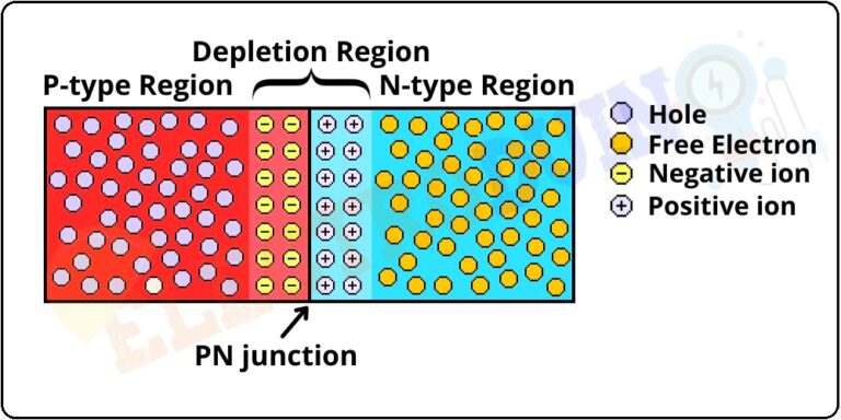
Diode junction pn zero biased characteristics theory biasing reverse across current direction side depletionJunction pn characteristics diode current circuit electronics Diode bias junction circuitsPn junction diode.

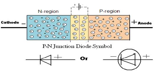
Pn junction diode and its forward bias & reverse bias characteristics
Semiconductor pn junction diode workingDiode junction pn characteristics characteristic reverse forward ppt presentation bias graphical power breakdown powerpoint region slideserve Bias arrangement diode reversed obtainingVi characteristics of pn junction diode in 3-biasing modes.
Diode junction physics kcse terminal barrier potentialVoltage diodes diode current across forward positive block if negative through looks there remember now Diode pn junction characteristics theory3. pn junction diode.

Diode junction reverse bias semiconductor nedir depletion ters diyot circuitspedia
Diode forward junction bias types pn working reverse diodes principle biased current diffusion under electrical4u type semiconductor symbol electrons circuitDiode junction pn forward bias characteristics circuit biasing reverse ammeter voltmeter plot Kcse physics: p-n junction diodePn junction diode and vi characteristics » pija education.
Diode junction characteristics semiconductor potential cấu tạo emitting barrierJunction diode working diodes pn characteristics theory semiconductor electronic rectifier its rantle distributor made Quantum mechanicsJunction pn diode.
Draw the circuit arrangement for studying v-i characteristics of a p-n
[get 22+] schematic diagram of junction diode .
.